Analog Engineering Fundamentals
Est. read time: 12 minutes | Last updated: July 17, 2026 by John Gentile
Contents
- Physics of Electrical Circuits
- Direct Current Circuit Analysis (DC)
- Alternating Current Circuit Analysis (AC)
- EM
- Components
- Designing Circuits
- References
Physics of Electrical Circuits
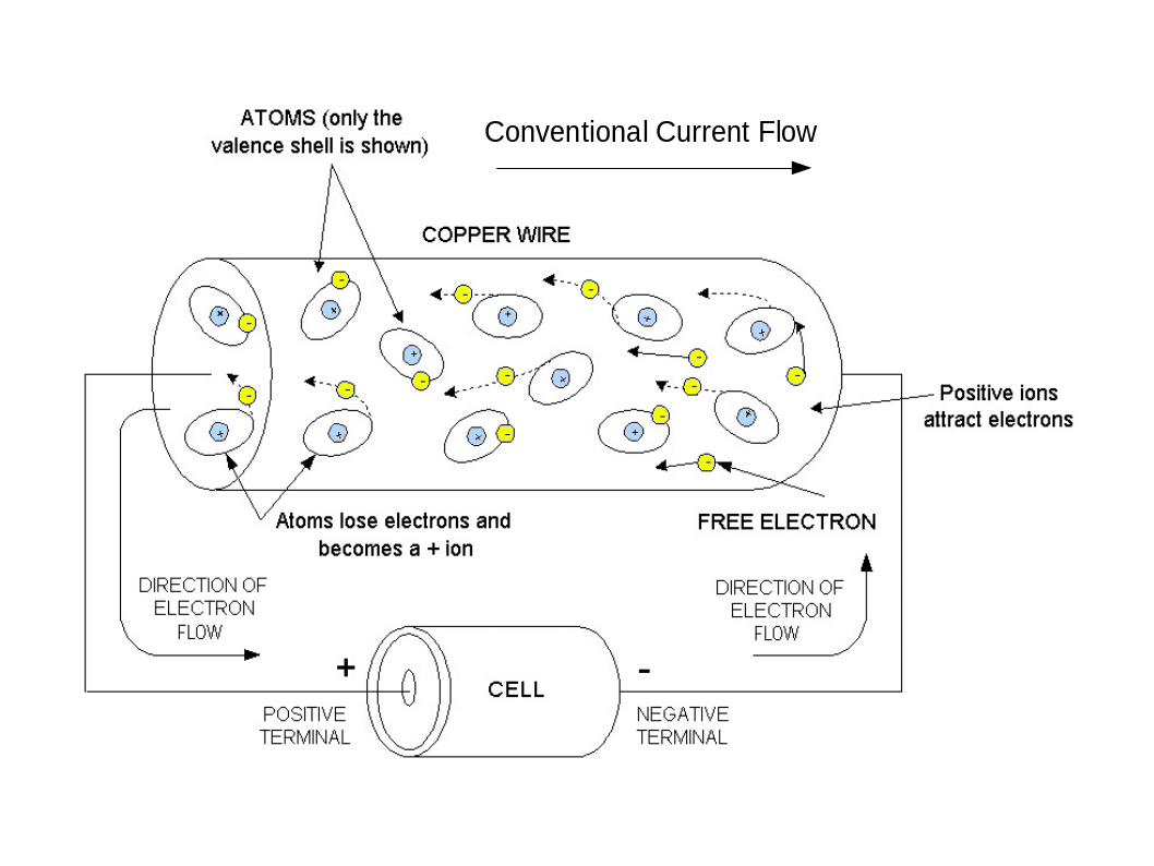
Fundamentally, there is the property of matter Charge which measured in Coulombs (C). Charge is directly related to one of the fundamental building blocks of matter, the electron; the charge of an electron (e) is negative and has a magnitude of .
Ohm’s Law
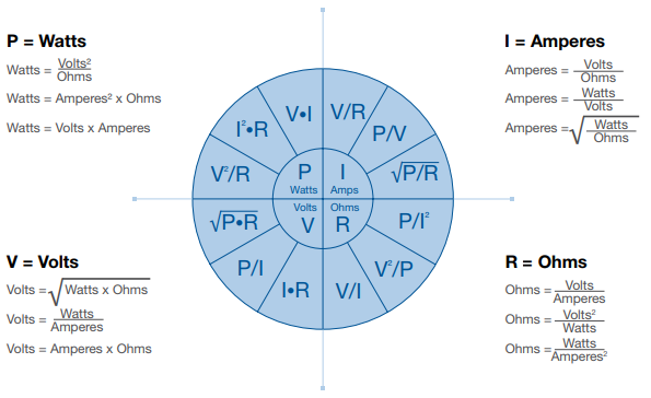
The fundamental, omnipotent equation in Electrical Engineering is Ohm’s Law which shows the relationship between the resistance (), voltage () and current () through an electrical path: $$ V = I*R $$ There are many different relationships that form from this:
Direct Current Circuit Analysis (DC)
For reference when specifying a DC circuit, use capital letters for voltage (), current () and resistance ().
KCL
Alternating Current Circuit Analysis (AC)
For reference when specifying an AC circuit, use lower case letters for voltage (), current () and resistance ().
Impedance
For impedances connected in series, the current through each is the same so the total impedance is the sum of each:
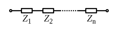
$$ Z_{eq} = Z_{1} + Z_{2} + \cdots + Z_{n} $$ $$ R_{eq} + jX_{eq} = (R_{1} + R_{2} + \cdots + R_{n}) + j(X_{1} + X_{2} + \cdots + X_{n}) $$
For impedances connected in parallel, the voltage across each is the same, thus the inverse equivalent impedance is the sum of the inverses of each impedance:
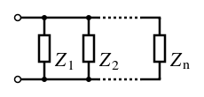
$$ \frac{1}{Z_{eq}} = \frac{1}{Z_{1}} + \frac{1}{Z_{2}} + \cdots + \frac{1}{Z_{n}} $$ A simplified version for the two element case is: $$ Z_{eq} = \frac{Z_{1}Z_{2}}{Z_{1}+Z_{2}} $$
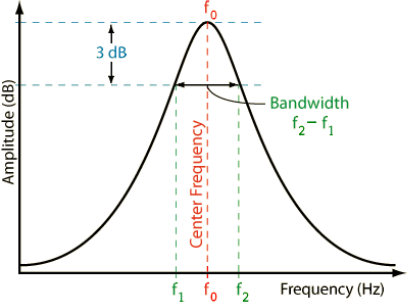
RLC Resonant Circuits
Quality factor is the ratio of energy stored to energy dissipated in a component or circuit: $$ Q = \frac{E_{stored}}{E_{dissipated}} $$
The less loss in a device the higher it’s quality factor. can also be determined by measuring the frequency response such that where is the 3dB bandwidth of the response:
Bode Plots
Bode plots are logarithmic graphs used to show magnitude (in dB) and phase response (degrees or radians) plotted over frequency ( or ). They can be measured in a real circuit, mathematically derived given a transfer function, or analyzed using CAD/SPICE software for a given circuit.
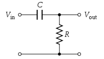
Drawing Bode Plot Manually
For quick response analysis of a given circuit it’s useful to be able to quickly draw the bode plot and transfer function. For example, given the following RC filter:
EM
Electromagnetic (EM) waves behave like all other waves:
- They can be continuous or happen in short bursts
- They propagate in some medium over time and attenuate as they propagate
- They can be absorbed or reflected
- Their paths can be guided
Transmission Lines
Application Examples
- When an ideal driver transmits a voltage into a high-impedance (open) receiver
- Almost all signal is reflected back creating a 2x driven amplitude (i.e. a 2.5Vpp driver will see a 5Vpp signal amplitude into an open receiver) on the line and, in the ideal case, the signal oscillates back and forth indefinitely
Components
Common Component Factors
- Power Rating: depending on the physical size and composition of the component, the power rating is indicative of how much power it can dissipate. Generally, a larger package can handle more power due to a larger surface area. It is generally not advisable to operate right at the nominal power rating of a part and instead operate with some margin due to component derating (see below).
- Working/Nominal Maximums: maximum DC or AC (rms) voltage or current that can be continuously applied to the component.
- Absolute Maximums: maximum DC or AC (rms) voltage or current that can be tolerated by the component, usually for a very short period of time. Never design to absolute maximums, always reference the working specifications and leave margin. – Dielectric Withstanding Voltage: max voltage that can be applied to component before dielectric breakdown occurs (meaning the insulator is no longer effective and becomes electrically conductive, which can be a safety issue or general failure)
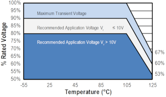
- Component Derating: most parts will show one or more curves expressing the relationship between some independent variable (e.g. temperature, voltage, current, etc.) and the dependent variable as some suggested derating of an otherwise nominal specification (e.g. rated power handling, maximum input current, etc.). These are critical to pay attention to when designing a system that may be in an environment where these bounds change the specifications significantly; for example derating a certain capacitor could mean limiting the maximum input voltage to the part given an application need to operate in a hot ambient temperature:
- Reliability: the probability that the component will fail, or not meet specifications, can be shown as the Mean Time Between Failures (MTBF), failure rate per hours of operation or other statistical measurements. Reliable electronics design is a deep subject and thus has its own page.
- Temp Coefficient: the “tempco” of a device is a measure of the variation of a given specification for a given change in temperature from where the specification was recorded. For example, a resistor with a temperature coefficient of resistance (sometimes shown as TCR) of 100 ppm/°C with a specified resistance of 10kΩ at +25°C will change 0.1% with a 10°C change in temperature. Generally, components with low tempco’s are beneficial as a design varies less over temperature.
- Tolerance: usually shown as a percentage of max deviation of a component from the nominal specification under nominal circumstances (e.g. same temperature and voltage as specification). For example a capacitor with 1% tolerance usually means that any capacitor used- when measured under nominal conditions- should fall within ±1% of the nominal capacitance. Component manufacturers can achieve a certain tolerance by careful material selection or by “binning” where components are tested and then bucketed into groups that meet a certain threshold. Generally, the tighter the tolerance of a component, the more expensive it will be (holding all other factors the same).
- Standard Values: for commonality between vendors and component manufacturers, standard values have been adopted for resistors, inductors and capacitors, given a certain tolerance bin. The values follow a logarithmic progression determined by the EIA E Series: $$ value = D * 10^{\frac{i}{N}} $$ where is the decade multiplier (10, 100, 1k, etc.), is the tolerance series (e.x. 1%=96, 5%=24, 10%=12) and . Thus for 10% resistor parts in the 1k decade, the standard values are: 1kΩ, 1.2kΩ, 1.5kΩ, 1.8kΩ, 2.2kΩ, 2.7kΩ, 3.3kΩ, 3.9kΩ, 4.7kΩ, 5.6kΩ, 6.8kΩ, and 8.2kΩ. It can also show that the higher the tolerance bin, the more value options available. Standard values are another factor in design decisions or part value selection since arbitrary values generally cannot be used; for instance, my calculation of a voltage divider calls for a 1.8725kΩ resistor but given standard values (and other factors like stock on hand, supplier/vendor availability, BOM cost, etc.) it’s most likely OK to use the standard 1.8kΩ part.
Resistors 
Resistors resist or limit the flow of electric current in a circuit. They are commonly used for:
- Voltage dividing
- Current limiting
- Energy absorption
Resistor Types
Resistor come in three main types:
- Fixed Resistors: where the one stated value of resistance is not intended to change. It’s most common that resistors are packaged individually however there are cases where an array makes sense:
- Resistor Networks: ResNets are an array, or multiple, resistors in a single package and are good for applications needing multiple resistors in close proximity (e.x. voltage dividers, resistor ladders, pull-up/downs for digital I/O, etc.) while also benefitting from better tracking (e.g. same manufacturing process/lot or substrate used leading to less variation between resistors).
- Variable Resistors: where the resistance value is changed via some mechanical mechanism (e.x. potentiometers and rheostats)
- Non-Linear Resistors: where the resistance value changes significantly with applied voltage (varistors), temperature (thermistors) or light (photoresistors)
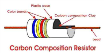
Resistors come in a variety of composition types:
- Carbon: older, low cost, terrible tempcos but can handle high peak power
- Thin/Thick/Metal Film: modern, tighter tolerances, generally good noise and high-frequency performance, smaller package sizes
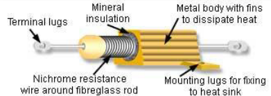
- Wire Wound: made for very high power applications though drawback is in size and inductance (since wire wounds act like an inductor)
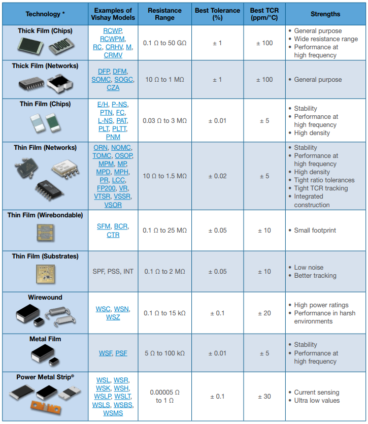
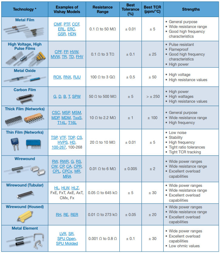
Resistors also can come in surface mount (SMT) or through-hole (TH) form factors with these different compositions:
Non-Idealities
Ideally a resistor has a constant impedance from DC to daylight (frequency independent) however, due to package type and how the signal propagates through the internals of the resistor, a resistor will look capacitive at high-frequency (lowering effective impedance), and then at even higher frequencies, start to look inductive (higher effective impedance):
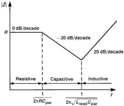
These non-idealities need to be considered for high-frequency or precision designs.
Noise
Resistors exhibit Johnson-Nyquist Noise which is caused by thermal agitation of charge carriers within the resistor. This noise is independent of applied voltage but rather dependent on temperature and bandwidth. Johnson-Nyquist Noise is present, and has constant power spectral density, across frequencies (approximately white noise) and is defined by: $$ v_{noise} = \sqrt{4 k T R B} \xrightarrow[noise]{current} i_{noise} = \sqrt{\frac{4 k T B}{R}} $$
Where is Boltzmann Constant (about ), is absolute temperature in Kelvin, is resistance Ohms and is bandwidth in Hz. Given nominal characteristics (e.g. room temperature and Boltzmann Constant), the rule of thumb noise voltage is: $$ V_{rms} = 1.3 \times 10^{-10} \sqrt{RB} $$
Bandwidth is not a single frequency but rather a range of frequencies (hence Band- width) that is relevant to the application of noise analysis. This also means that the frequency of operation, or center frequency for instance, does not matter since the noise is constant throughout the frequency spectrum; again, what matters is the bandwidth of operation. For example the Johnson-Nyquist noise power spectral density (and resulting noise voltage) with a bandwidth of 1 MHz is equivalent whether the band is centered at 10 MHz or 1 GHz.
Ideal inductors and capacitors do not exhibit noise, but their non-ideal/real-life models do exhibit resistance in some fashion; however, one can generally ignore these noise sources since the equivalent resistances present are typically negligible.
Since noise from different sources (e.g. two discrete resistors in series) are uncorrelated and independent (it’s statistically unlikely that the random fluctuations of both resistors will be exactly the same- in power and in phase at any given time- even at the same temperature or process), the noise must be added in RMS: $$ v_{noise total} = \sqrt{(v_{noise 1})^{2} + (v_{noise 2})^{2}} $$
Tempco
Resistors follow similar tempco guidance as other components and generally increase in resistance as temperature increases. However, some resistors are specifically designed with large and negative tempcos- like thermistors- to better serve a specific application like temperature compensation or measurement.
Voltage Coefficient of Resistance (VCR)
Resistance of a part can change with applied voltage though this property is often not specified for general low/standard voltage work. High-voltage (HV) resistors, though, will show the VCR as it is a concern for HV work.
Inductors 
Inductors are reactive devices that store energy in a magnetic field when current flows through and oppose changes in current through them. Commonly they are used in:
- Power supplies
- Tuned circuits & filters
- Transformers
Construction
Since the inductance of most solenoid inductors follows the equation: $$ L = \frac{N^{2}\mu_{r}\mu_{0}A}{l} $$
Manufacturers have worked to increase the inductance of parts by either:
- Increasing the number of turns ()
- Increasing loop area ()
- Decreasing the length ()
- Using new/ferrous core materials to increase relative permeability
Non-Idealities
Ideally an inductor has an impedance which follows the equation however due to resistive losses and inter-winding capacitance (self-resonance) an inductor will start to behave as a capacitor past its self-resonant frequency and decrease in impedance.
Capacitors 
Capacitors are reactive devices used to hold charge in an electric circuit and are commonly used for:
- Energy storage
- High-frequency paths
- DC-blocking
- Decoupling
Capacitors can be bi-directional (placed in either direction) or polarized (where the cathode is shown as a “+” in the schematic symbol and is polarity sensitive) like in electrolytic capacitors.
Construction
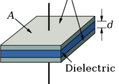
Capacitors are still based on the parallel-plate model above where: $$ C = \frac{k \epsilon_{0} A}{d} $$ so to reduce package size but increase capacitance, manufacturers have played with each variable:
- Increased area () by using multi-layer design techniques
- Reduced plate distance () by reducing the voltage rating (otherwise dielectric breakdown or arcing could occur)
- Utilize advanced dielectrics in between to increase the coefficient
Non-Idealities
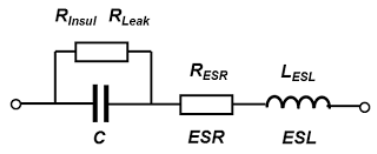
Ideally a capacitor acts as a purely reactive device and follows the well-known capacitor equation for it’s impedance as . However, mainly due to package inductance and resistance, at some higher-frequency of resonance, a capacitor will start having higher impedance as frequency increases as it becomes more inductive. A real capacitor acts like a notch filter.
Diodes 
The basic operation of a diode is to conduct current in one direction while blocking current in the opposite direction (asymmetric conductance); the ideal diode has zero resistance in one direction and infinite resistance in the other. Semiconductor diodes are made with a p-n junction.
There are many different types and constructions of diodes for many applications:
Zener
Schottky
TVS
LED
BJT
The bipolar junction transistor (BJT) were of the first semiconductors (solid state devices) developed to replace old vacuum tubes for purposes of amplification. Solid state devices solved a lot of the issues with large, high-voltage tubes and led to integrated circuits due to their ability to operate at much smaller sizes. However, tubes and other thermionic devices are still better suited for very high power and high frequency operation (e.g. 100kW Klystron or 1 MW Traveling Wave Tube) for purposes of Radar or other applications.
The bipolar in the name is in regards to the two complimentary doped semiconductors used to create the transistor- two PN junctions, almost like two diodes squished together at either end depending on the type. However, the devices are unipolar in that they are intended to operate actively with a certain polarity of input voltages:
- NPN: requires
- PNP: requires
This also means signals like zero-offset sinusoids cannot just be plugged into the base of either (since sinusoids oscillate between positive and negative voltages); for this reason, most AC BJT circuits require a bias circuit to bring the DC offset/operating-point of the signal within the proper range required.
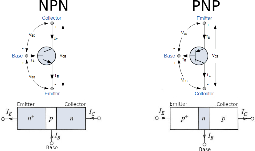
A mnemonic key to remember the difference in symbology is NPN has the arrow Not Pointing iN (where as PNP has the arrow pointing towards its base).
Transistors can operate in three main modes:
- Cutoff
- Saturation
- Active
Transistor design is a special topic in analog design and covers many facets of amplifier circuits and even integrated circuit design.
BJT Component Characteristics
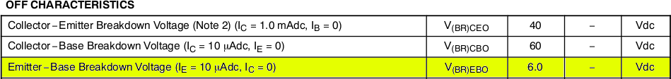
There are a couple things to note when dealing with real (non-ideal) BJTs, for example for a 2N3904 device:
- Breakdown Voltages: While BJTs can usually handle a fairly high potential at the collector terminal, the base terminal should not be reverse biased too far; for instance, in the
2N3904, if the emitter is grounded, the voltage at the base should not go below or one risks breaking the device:
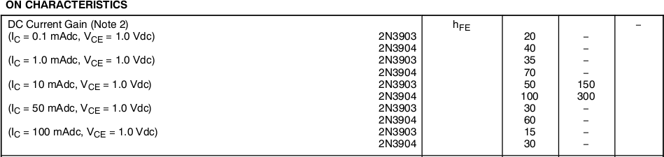
- Beta: the gain of the BJT is very variable (almost 3x between minimum and maximum values!) and depends on a lot of factors, one mainly being the collector current present (a higher collector current will often lead to a larger ), so don’t rely too much on a single beta value without giving much room for margin:
- Thermal Performance: besides the usual derating curves and operating points for given system temperatures, BJTs also can suffer from a phenomenon known as thermal runaway; when BJTs start to heat up, temperature dependent characteristics cause even more power to be dissipated, which in turn, cause even more heat. For instance with increased temperature, base-emitter voltage decreases (), increases, and emitter current increases (in aforementioned Shockley diode equation, saturation current - though small- nearly doubles ever +10°C). Thermal junction resistance is usually given to show the increase in temperature of the device for a given power dissipation through the device; for instance, the
2N3904has a (junction-to-Ambient, means no heatsink, just nominal air flow) of , which means for every Watt of power dissipated, the part will increase temperature by roughly 200°C.
Designing Circuits
Reference Designs
Modeling & SPICE
SPICE is an acronym for Simulation Program with Integrated Circuit Emphasis which was originally made to model ICs and their behaviors. A popular tool is LTSpice (developed by Linear Tech which is now owned by Analog Devices) which has a simple interface and lots of capabilities such as Monte Carlo analysis (useful for modeling impact of component tolerances), parametric analysis and noise analysis. Note the Windows version is the most full featured so if installing on MacOS or Linux use Wine Windows emulator. Multisim is another tool from NI.
Some main analysis types that are commonly used are:
- DC: computes the DC operating point of a circuit given system conditions (e.g. input voltages and DC characteristics) and is required for other analysis types.
- AC/Small Signal: performs frequency sweeps across the circuit to do frequency domain analysis, however care should be taken since results are linearized about given DC operating point. Valid for small signal analysis.
- Transient/Time Domain: simulation done over a time period to see effects of given events, for example power supply transient response to load step. Valid for large signal analysis.
- Noise Analysis: simulation of system effect of various noise sources in schematic.
LTSpice Tricks
- Change device model parameters: One way to quickly change a device’s model parameters is the AKO method; for instance, to change the forward Beta of a
2N3904BJT to 120, the below SPICE directive can be made, and then for the transistor to be changed, “Pick” a new part and enter the name used (e.g.my_2N3904):.model my_2N3904 AKO: 2N3904 (Bf=120)Further, if you want to step through a list of parameters to change, one could do:
.step param beta_step LIST 70 120 210
.model my_step_2N3904 AKO: 2N3904 (Bf={beta_step})
References
Maintained by John Gentile • Found a problem on this site? File an Issue
This work is licensed under a Creative Commons Attribution 4.0 International License.![]()