DSP Design
Est. read time: 9 minutes | Last updated: July 17, 2026 by John Gentile
Contents
- Overview
- Basic Operations
- Integer and Fixed-Point Operations
- Processing Architectures
- Tools
- References
Overview
For digital implementation languages, see VHDL and Verilog page. Also for background/theory on following DSP implementations see the DSP Page. Most of this page has references and example code for VHDL, though the underlying concepts apply to all Hardware Description Languages (HDL), as the architectures are applicable to many digital processing & hardware accelerated systems, like FPGAs, ASICs, and even SW-programmable DSP processors.
Why Learn Low-Level DSP Design for Digital Systems?
Knowing low-level design & implementation of Digital Signal Processing (DSP) for Digital Systems can be valuable for a number of applications. For instance high-level synthesis (HLS) has made great progress in recent years, and can lead to very quick implementations, however it is not universally applicable to every scenario. HLS may not be as performant/resource-efficient as HDL crafted “by-hand” either.
Similarly, it’s important to realize from the beginning that there are scenarios where just directly porting an algorithm to an FPGA is not faster than the same algorithm running in software (SW) on a CPU. For one, FPGAs are generally clocked much slower than CPUs (e.x. FPGA fabric runs in the 100’s of MHz vs modern CPUs in the GHz range). Second, SW compilers- and processing libraries with optimized code- have become great at creating applications that efficiently use modern computer architecture features such as cache memory, parallel-processing/threading and SIMD vector extensions.
Put simply, FPGAs and Digital Hardware offer a different processing & design paradigm than SW so there are some basic tenets to keep in mind when designing for high-throughput processing performance:
- Design for data and process parallelism over a single-threaded-execution model: due to completely distinct logic blocks, high-throughput digital implementations (e.g. sample rate greater than synchronous, digital clock rate) should aim to process multiple samples of data per clock cycle in parallel, rather than a single sample per cycle (e.x. we can process data at 1 GS/s if we can process 4x samples in parallel, per clock cycle, and only run at a 250 MHz digital clock rate). Conversely, we can reuse- or “fold”- digital resources when the sample rate is less than the clock rate; for instance, an 8-tap filter need only use one multiplier if the clock rate is at least 8x the input sample rate.
- Know the strengths & weaknesses of data movement to, from and within Digital Systems/SoCs: moving data to/from an accelerator (e.g. FPGA) from/to main memory (e.g. over DMA) can be costly in terms of latency for some applications compared to SW algorithms which are cache-optimized; even in DMA offload blocks which have optimizations like pre-fetching descriptors, data still has to move from memory to the digital logic and back. However in other applications, Digital Systems like FPGAs are valuable in that they can directly interface with sensors and other system I/O; here, processing can be brought to the data, rather than moving data to the processing.
- Think in data flow rather than sequential processing: as an extension to data parallelism, digital HW algorithms can easily implement processing pipelines which can perform different stages of processing concurrently (e.g. at the same time- rather than waiting for the current processing chain to finish before starting the next processing chain). Keep the execution pipeline full to achieve maximum throughput of your algorithms. Dataflow, or Stream Processing, can be applied to systems which exhibit:
- Compute Intensity: where there is a large ratio of the number of arithmetic operations per I/O or global memory reference.
- Data Parallelism: which exists in a kernel if the same function is applied to all records of an input stream and a number of records can be processed simultaneously without waiting for results from previous records (e.x. digitized RF samples in a wireless processing system).
- Data Locality: a specific type of temporal locality where data is produced in a stream, with intermediate streams passed between kernels.
- Understand the entire system to apply the right tool at the right time: Similar to the applicability of data movement, there may be scenarios where parts of your algorithm should be done in software, while other parts are accelerated by FPGA fabric; often this is done in tandem where the FPGA & CPU are working simultaneously. FPGAs are not the answer for every application, so the wise Digital Engineer should recognize, and understand, processing software to determine an overall processing architecture given system constraints (e.x. Size, Weight and Power, plus Cost (SWaP-C)). For instance, high-core-count CPUs with wide, modern SIMDs (like AVX-512) can process high-bandwidth signals like DVB-S2 in real-time. However, these server-class CPUs can burn 200W+ of TDP. Compare this to highly-integrated FPGA SoCs like the AMD-Xilinx RFSoC which can process multiple channels, at multiple GS/s, with control SW and 100GbE at package power draws measured in the tens of Watts. Or with even lower SWaP-C constraints, SDRs like the ADI ADALM-PLUTO can process 20 MHz of instantaneous of BW on just USB power.
Basic Operations
Numeric Representations
Integer Representations
There are a few different integer number representations when working with digital logic:
- Unsigned: the direct numeric representation of a binary number, assuming no sign or negative numbers. For an bit unsigned integer, the range of representable values is .
- Signed: there are two main representations for integers containing both negative and positive values:
- One’s Complement: the one’s complement of a number (or negation of a signed integer) is simply the negation (inversion) of all bits (see table below). It is not very popular due to issues such as the offset representation of -1, negating zero gives another -0 pattern, and less simplicity with carry logic. One’s complement has a range of .
- Two’s Complement: Two’s complement is the prevailing signed integer representation used in digital logic and computer systems. Besides not having the same issues as One’s complement, arithmetic logic & operations are also identical for use with unsigned and two’s complement numbers, so designs can be shared between numeric representations. The two’s complement of a number is essentially the bitwise inverse of a number, and then a one added to that. Two’s complement has a range of
| Binary Value | One’s Complement Interpretation | Two’s Complement Interpretation | Unsigned Interpretation |
|---|---|---|---|
| 00000000 | 0 | 0 | 0 |
| 00000001 | 1 | 1 | 1 |
| 01111110 | 126 | 126 | 126 |
| 01111111 | 127 | 127 | 127 |
| 10000000 | -127 | -128 | 128 |
| 10000001 | -126 | -127 | 129 |
| 10000010 | -125 | -126 | 130 |
| 11111110 | -1 | -2 | 254 |
| 11111111 | -0 | -1 | 255 |
VHDL Integer Type
Note that VHDL has a standard integer type, however caution should sometimes be used as most synthesis tools infer full 32-bit wide resources for unconstrained integer signals. Therefore, when dealing with integers it’s best to:
- Constrain the intended range of an integer signal:
signal my_int : integer range -4 to 7; - Primarily use integers as constants or literals:
Y <= X + 7;
Type Conversions
Since VHDL is strongly typed, integer types need to be converted to and from each other, as well as between std_logic_vector, with the following functions:
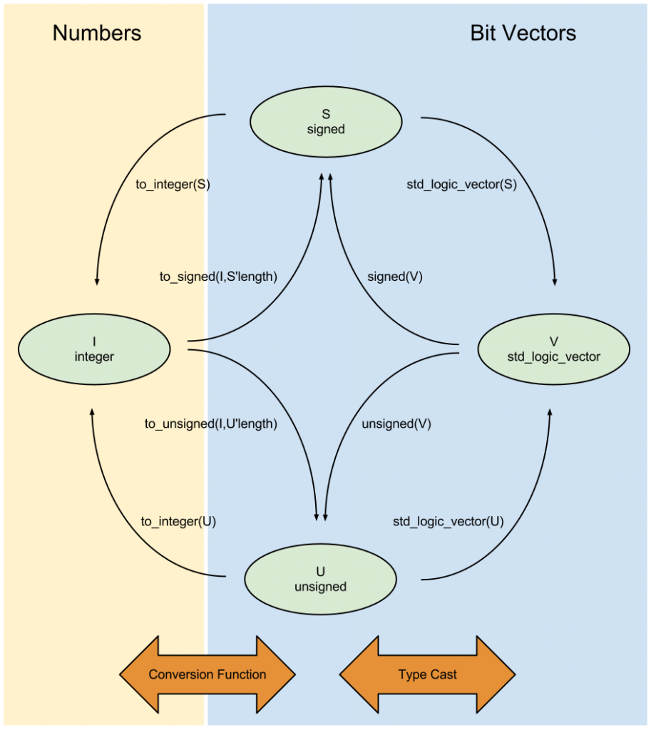
For instance, to convert a std_logic_vector signal A to a signed integer signal B:
signal A : std_logic_vector(3 downto 0) := "1111";
signal B :           signed(3 downto 0);
-- ...
B <= signed( A ); -- B = -1 (decimal)
Fixed Point
Floating Point
Integer and Fixed-Point Operations
Addition and Subtraction
In VHDL, addition operands on the right-hand side must be equal in size as the assignment result on the left-hand side; what this means is that, in order to accommodate any overflow from the addition or subtraction operation, it’s best practice to have the output result to have a bit width equal to the largest operand, plus one. Using the numeric_std resize(arg, new_size) function, signed and unsigned types can be easily resized, with sign extension, to create the necessary intermediate operands for bit growth:
signal A : signed(5 downto 0); -- 6 bit
signal B : signed(3 downto 0); -- 4 bit
signal C : signed(6 downto 0); -- length = max_length(A,B) + 1 = 7 bit
-- ...
C <= resize( A, C'length ) + resize ( B, C'length );
Multiply
When multiplying two integers together, the output bit width is the sum of each operand’s bit width:
signal A : signed( 7 downto 0); -- 8 bit Input
signal B : signed( 3 downto 0); -- 4 bit Input
signal C : signed(11 downto 0); -- 8 + 4 = 12 bit Output
-- ...
C <= A * B;
Complex Multiply
Direct Implementation
Given two complex signals of and , the complex product of can be implemented directly using four multipliers and two add/sub operations: $$ p_{r} = a_{r}b_{r} - a_{i}b_{i} $$ $$ p_{i} = a_{r}b_{i} + a_{i}b_{r} $$
Reduced Resource Implementation
A reduction in multiplier resources can be made by rearranging common terms in the real and imaginary product so that only three multipliers are needed: $$ p_{r} = a_{r}b_{r} - a_{i}b_{i} = a_{r}(b_{r}+b_{i}) - (a_{r} + a_{i})b_{i} $$ $$ p_{i} = a_{r}b_{i} + a_{i}b_{r} = a_{r}(b_{r}+b_{i}) + (a_{i} - a_{r})b_{r} $$
Three pre-combining adders are necessary (which in Xilinx DSP48 slices are built-in) which also results in increased multiplier word length. Another tradeoff is that, since the three multiplier utilizes more slice resources, the three multiplier design has a lower maximum achievable clock frequency than the four multiplier implementation.
Transcendental Functions
Transcendental functions are simply functions which cannot be completely expressed in terms of algebraic operations (e.g. addition, subtraction, multiplication, division, raising to a power or root extraction). For example, exponential, logarithmic and trigonometric functions are transcendental.
CORDIC
CORDIC (COordinate Rotation Digital Computer) was developed by Jack Volder in 1959 as an iterative algorithm to convert between polar and cartesian coordinates using shift, add and subtract operations only.
- Thus the algorithm is very popular since it requires no inherent multiplications and can therefore be used to save computing resources or be used on low power devices such as microcontrollers.
- Can also compute hyperbolic, linear and logarithmic functions as well
- CORDIC algorithms generally produce one additional bit of accuracy for each iteration taken
Processing Architectures
Data Flow and Control in Digital Circuits
Since digital systems, like FPGAs, flow data through DSP stages, and most DSP processes assume a synchronous, constant flow of sample data, there are a couple avenues to handle the control flow:
- Match the processing clock rate (e.g. FPGA synchronous clock) exactly to the input data stream, such that when globally enabled, each clock-tick of samples are guaranteed valid. This is useful in digital systems where the source/sink of samples external to the FPGA (e.x. ADC/DAC) can drive the clock directly (source-synchronous clocking).
- In systems where we can’t be source-synchronous (e.g. the DSP stages are clocked much higher- or can process faster- than incoming data samples, or clock rates are slightly different/asynchronous between source and processing), there exists times where data is not valid but processing is ready for the next sample (in AXI parlance,
tvalid = 0of sample source buttready = 1of processing stage). To deal with these gaps, it may be necessary to buffer incoming data (FIFO) and/or have globalenablesignals to start/stop the entire processing chain.- In DSP processing, where there are feedback/feedforward stages that have tight sample-to-sample timing dependence, this model works better than each stage having independent
ready/validsignaling (though globalenablesignal may have high fanout in digital logic). With individualready/validsignaling, some paths of processing may continue to propagate while other parallel paths are stalled; in the case of a fedback signal, this could mean that the response is applied at the wrong time. - In systems where the dataflow is independent/serial, you could use
ready/valid(or justvalidin and out signals if you know that the processing will always keep up and never backpressure) between stages. For example in a modem receiver design, the major blocks, likematched filter -> timing recovery -> carrier recovery, could use interstageready/validsignaling between them, while the internals of a given stage (e.g. timing recovery which encompasses feedback loop filters and other parallel, timing-dependent stages) could use a globalenablesignal to keep data processing coherent.
- Note another reason to skip
readysignaling- if you know you won’t ever backpressure and can keep up with the input data stream- is to avoid needing to use skid buffers to optimally handle theready/validinteractions.
- In DSP processing, where there are feedback/feedforward stages that have tight sample-to-sample timing dependence, this model works better than each stage having independent
Kahn Network Descriptions
https://en.wikipedia.org/wiki/Kahn_process_networks
Systolic Arrays
https://en.wikipedia.org/wiki/Systolic_array
Tools
Device Primitives
To hit performance, cost, power, etc. goals, it’s critical to understand the processing architecture and hardware you’re targeting. For instance in CPUs, understanding the specific SIMD units available. Or for FPGAs, understanding the primitive blocks available and how to correctly utilize them (e.g. inference vs direct instantiation). Beyond IP blocks for interfacing (e.g. Ethernet) or memory (block vs distributed RAM), for DSP, vendors such as AMD-Xilinx provide DSP blocks in PL which are meant to handle common DSP tasks. It’s critical to understand the different features available to best utilize them.
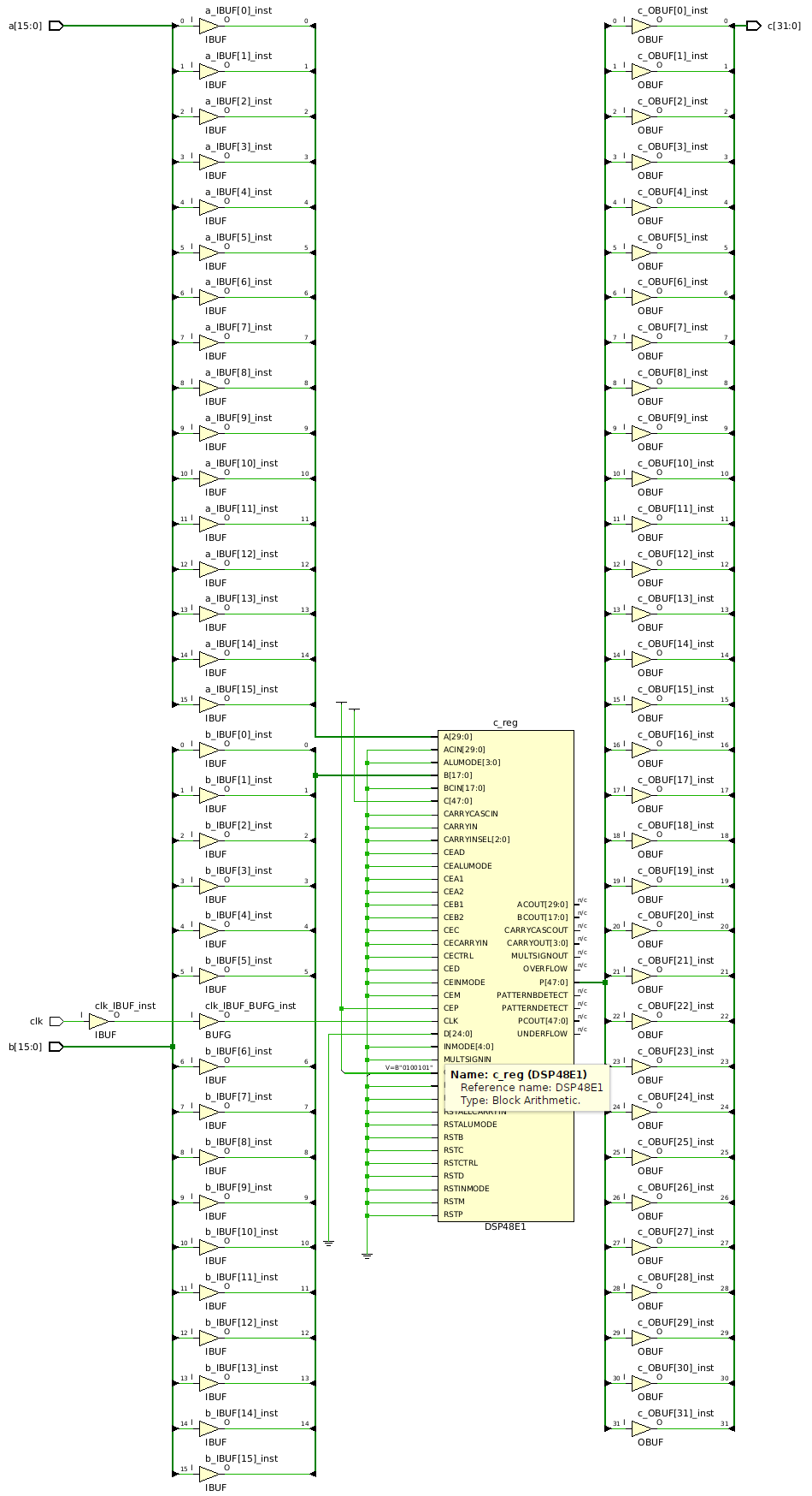
For example, a common DSP operation is the multiply-accumulate (MAC) operation, where a product is added to an accumulator, such as c += a * b. One way to target a DSP48 block is to either directly use the DSP48 macro and set the correct opcode, or to use inference (coding in a style that the synthesis tool will pick up the correct device primitive) which has the added benefit of being more portable than direct macro instantiation (similar to compilers with autovectorization capabilities vs directly coding intrinsics/assembly to target SIMD units). In this case, we can show two 16b inputs multiplied together and accumulated in a 32b accumulator, operating all in one clock cycle:
module test_mac(
    input  logic clk,
    input  logic signed [15:0] a,
    input  logic signed [15:0] b,
    output logic signed [31:0] c
);

  always_ff @(posedge clk) begin
    c <= (a*b) + c;
  end
endmodule
We can see that the synthesis tool (in this case Vivado 2022.2) correctly infers the DSP48 in a multiply-accumulate mode by looking at the synthesis report:
DSP Report: Generating DSP c_reg, operation Mode is: (P+A*B)'.
DSP Report: register c_reg is absorbed into DSP c_reg.
DSP Report: operator c0 is absorbed into DSP c_reg.
DSP Report: operator c1 is absorbed into DSP c_reg.
...
DSP: Preliminary Mapping Report (see note below. The ' indicates corresponding REG is set)
+------------+-------------+--------+--------+--------+--------+--------+------+------+------+------+-------+------+------+
|Module Name | DSP Mapping | A Size | B Size | C Size | D Size | P Size | AREG | BREG | CREG | DREG | ADREG | MREG | PREG |
+------------+-------------+--------+--------+--------+--------+--------+------+------+------+------+-------+------+------+
|test_mac    | (P+A*B)'    | 16     | 16     | -      | -      | 32     | 0    | 0    | -    | -    | -     | 0    | 1    |
+------------+-------------+--------+--------+--------+--------+--------+------+------+------+------+-------+------+------+
This is also seen by viewing the synthesized schematic showing the DSP48 block directly tied to the inputs and outputs:
RFNoC
References
Maintained by John Gentile • Found a problem on this site? File an Issue
This work is licensed under a Creative Commons Attribution 4.0 International License.![]()